


UPSC Relevance
GS-3: Science & Technology – Electronics advancements, silicon photonics
GS-3: Economy – Innovation, cost-efficient manufacturing
GS-3: Infrastructure – Impact on digital communication, data centers
Key Highlights
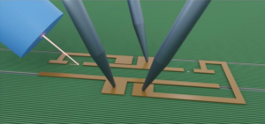
From Electrons to Photons
Conventional chips rely on electrons for data transfer.
Researchers have now integrated miniature lasers onto silicon chips, enabling photon-based computing. This shift to silicon photonics offers faster speeds, higher energy efficiency, and greater data capacity with minimal heat loss.
Breakthrough Innovation
A US-Amber Wave Systems team, published in Nature, grew tiny lasers directly on silicon wafers. They achieved a fully monolithic laser diode on a standard silicon chip—a pioneering feat.
Scientific & Technical Details
Why It’s Groundbreaking
Resolves atomic crystal mismatches between laser materials and silicon.
Previous methods required separate laser attachments, which were costly and less efficient.
Laser Mechanism
Lasers function by exciting electrons to emit photons as they drop energy levels. Indium gallium arsenide, layered over etched silicon nano-ridges, traps defects to ensure laser performance.
Production Process
Involves layering indium gallium arsenide, phosphide, and gallium phosphide.
Chips are compatible with standard CMOS semiconductor lines, enabling mass production.
Significance
Speed & Efficiency: Photonic data transfer is faster and reduces energy waste.
Compact Design: Photonic chips replace bulky laser components, enhancing device power and size.
Heat Management: Operates effectively at room temperature, cutting cooling costs.
Applications & Impacts
Data centers: Lowers energy use and boosts transmission speeds.
Quantum computing: Supports optical processing advancements.
Telecommunications: Enables ultra-fast broadband connectivity.
Analysis & Way Forward
Compatibility with existing manufacturing ensures commercial scalability.
As computing needs grow, energy-efficient technologies like this are critical.
India’s semiconductor mission should invest in photonic chip R&D to lead in technological innovation.